| Columns Retired Columns & Blogs |
Bits is Bits? Page 8
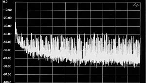
We now progress to an examination of simulated DAC errors due to band-limited interface jitter. Fig.36a shows the jitter-error spectrum for a 100% DAC reproducing a 0dBFS, 20kHz audio signal with an interface RC time constant of 40ns; the PLL cutoff frequency is set to infinity so that any jitter on the interface won't be attenuated before reaching the DAC. The error contains discrete frequency components rising from the noisefloor—this is because bandwidth-limited interface jitter can contain components that are well correlated with the audio signal (see "Interface Noise").
Footnote 36: Martin Colloms, Hi-Fi News & Record Review, March 1991, pp.69-71.
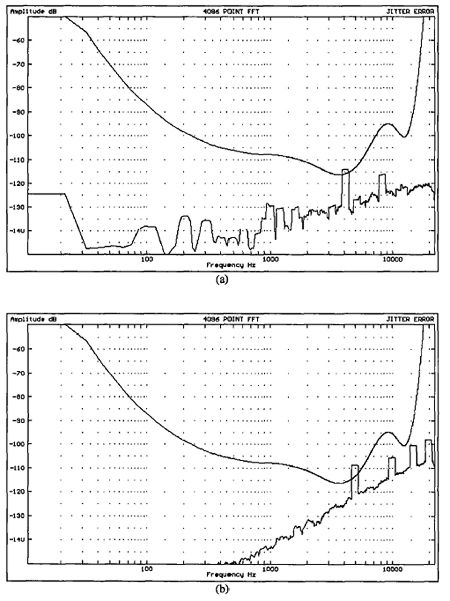
Fig.36 Simulated band-limited interface jitter errors with no PLL filtering: a) 20kHz at 0dBFS, 100% DAC, interface time constant 40ns (top); b) 9.8kHz at 0dBFS, impulsive DAC, interface time constant 50ns (bottom).
Fig.36b shows a similar simulation for an impulsive DAC fed a 0dBFS, 9.8kHz audio signal; in this case, an interface time constant of 50ns results in an audible error. Of course, most interface receivers will employ PLL filters such that interface jitter above the PLL cutoff frequency is attenuated. This results in the jitter error forming "skirts" around the audio signal; examples for 100% and impulsive DACs reproducing full-scale 7kHz sinewaves are shown in fig.37. The PLL second-order filter cutoff has been set to 1kHz, with the result that the interface time constant can be increased to 120ns before jitter audibility occurs. Finally, fig.38 compares the jitter errors from 100% and impulsive DACs, respectively, while replicating a 200Hz full-scale sinusoid from an interface with a 100ns time constant (the PLL filter is set to 1kHz, second-order). The higher jitter error from the impulsive model while reproducing low-frequency signals is clearly evident, an interesting result considering the claimed higher sensitivity of Bitstream DACs to digital interface quality compared to their multibit counterparts (footnote 36).
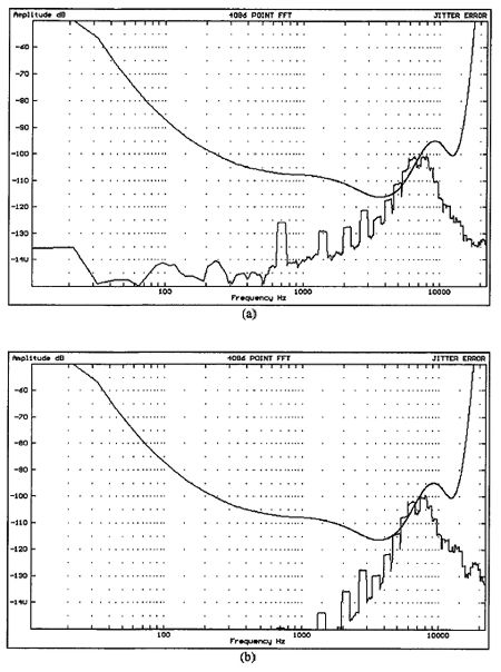
Fig.37 Simulated band-limited interface jitter errors with 2nd-order 1kHz PLL filter: a) 7kHz at 0dBFS, 100% DAC, interface time constant 120ns (top); b) 7kHz at 0dBFS, impulsive DAC, interface time constant 120ns (bottom).
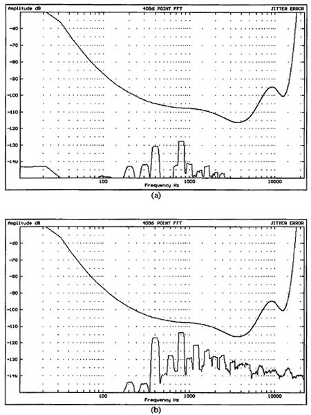
Fig.38 Simulated interface jitter errors with low-frequency, audio signal, 200Hz at 0dBFS, 100ns interface time constant, and 2nd-order 1kHz PLL filter: a) 100% DAC (top); b) impulsive DAC (bottom).
Clearly, the lower the PLL's bandwidth, the more wideband jitter the digital interface link can tolerate. Our simple audibility model has not considered masking due to the audio signal itself; when this is taken into account, it is evident that reducing the PLL break frequency has the additional benefit of narrowing the jitter-error skirt around the audio signal—hence making the skirt less audible. There is a clear analogy here to data-reduction systems in which efficient coding of audio signals places the error directly under the audio signal where, because of masking, it is least audible (footnote 37).
The worst case for interface jitter audibility is when the receiver PLL has a high-jitter bandwidth; several ADIC integrated circuits on the market have jitter bandwidths up to 5kHz (footnote 38). In the limit (no filter at all) white jitter noise of up to 180ps peak amplitude and even less sinusoidal jitter will not produce errors that rise above the audibility curve, more or less justifying the recommendations in AES11-1991. Similarly, we have seen that for no PLL filter, the interface time constant must be lower than 40ns or, equivalently, possess a bandwidth higher than 4MHz, a requirement which makes the performance offered by TosLink-type optical interface links marginal (footnote 39, footnote 40).
The revised professional interface standard AES3-1992 (footnote 41) stipulates a reasonable upper limit of 30ns on the 10-90% risetime for correctly terminated interface transmitters, corresponding to a time constant of 14ns. However, we have seen that time constants need to be minimized in each part of the interface (transmitter, link, receiver), and that observing sharp rise and fall times at one point in the chain does not guarantee waveform fidelity elsewhere. For example, our experimental receiver circuit suffers from a 65ns time constant associated with the ADIC IC used.
Reducing the Audibility of Interface Jitter Errors: We have shown that embedded clock jitter in a band-limited digital audio interface is fundamentally a problem due to the digital audio interface standard in its current form. In particular, the jitter signal is intimately linked with the Zero-One bit sum of the serially transmitted audio words; a lower Zero-One sum range would result in reduced jitter.
One way of lowering the sum using the present interface standard is to pad the unused bits in the auxiliary data and low-bit sections of each subframe (see fig.2). For example, with 16-bit audio words, the sum can be reduced from ±16 to ±8 by appropriately filling these unused bits according to the value of each transmitted audio word (footnote 42). A second option is to transmit one of the two audio channels supported by the interface out of phase, such that, for stereo program with a strong monaural component, the Zero-One sum is reduced.
However, although these techniques may reduce the absolute jitter level, we will still be left with the undesired high correlation between jitter and audio. In order to break this correlation, we must somehow randomize the sign structure of the transmitted bits, perhaps by modulating each bit sign with a known pseudo-random binary sequence, synchronized at the start of each interface block.
The AES/EBU-S/PDIF digital audio interface is now in widespread use; we are not likely to see a new interface standard welcomed by the majority of users for a considerable time. Accepting that jitter will occur in a band-limited interface, we must examine methods of reducing recovered clock jitter in receivers. Evidently the first step to take in minimizing interface jitter is to maximize the bandwidth of all components in the interface. However, there are limits to achieving high bandwidth at low cost, especially for long links, and conflicts with RFI may develop as rise and fall times become very fast.
Alternately, the audibility of interface jitter in a conversion process can be reduced by making the receiver PLL cutoff frequency as low as possible. But note that PLLs with extremely low cutoff frequencies may be compromised in other performance aspects, such as initial lock-on time and the frequency range over which lock is maintained. These problems can be overcome by employing two PLLs in series, where the first has high bandwidth and fast startup, and the second low-bandwidth module is switched into circuit after conditions have stabilized (footnote 43). Low loop bandwidths can be achieved while maintaining wide lock range by using random access memory (RAM) to buffer the audio data before it is clocked out to the converter unit.
A more fundamental solution to the problem of interface jitter is to locate a high-precision conversion clock inside the "receiver" (ie, DAC). This then creates the problem of how to match the transmitter and receiver data rates. One solution is to employ a RAM buffer for audio data where the rate at which the data is clocked out of the interface is under the control of the local clock (footnote 44). Enough memory must then be available to account for the long-term differences between the transmitted interface clock and the local oscillator frequencies. However, this is hardly an acceptable solution in a studio environment, where equipment must operate with identical sampling frequencies. A more general solution is to slave the receiver clock to the transmitter via a separate link, an approach adopted by Sony and Linn in their two-box CD systems.
Details concerning how to implement the additional clock interface vary, but perhaps the most sensible and universal approach is to provide a second independent digital audio interface output at the receiver, from which the transmitter can derive a clock signal (fig.39). This scheme is also compatible with the recommendations made in AES11-1991 1.
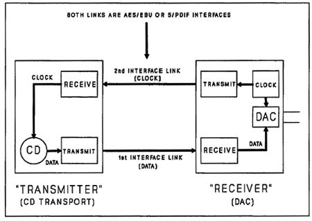
Fig.39 Proposed system connection for master clock at receiver utilizing two digital interface links.
Measuring Jitter in the Digital Audio Interface: The simulations presented above indicate that interface jitter may be a real problem in practical audio systems. How can we measure the effects of such jitter? In general, jitter errors in DACs will lie close to the noisefloor of the conversion process, resulting in two basic problems for measurement strategies:
First, there is the problem of resolution in the test instrument itself; since jitter errors are most easily revealed when exercising the test system with full-scale audio signals, then errors in the ADC of a digital measurement system, also excited to close to full scale, may well swamp those due to jitter in the test device.
Second, there is the problem of determining the source of measured errors. We have seen that jitter errors can contain both noise-like components and spectral lines, and that these can be confused with distortion and noise modulation due to DAC non-linearity. Noise-modulation tests in which the exciting audio frequency is chosen so that all DAC non-linearity falls on a limited number of FFT bins are perhaps the best-suited for revealing jitter errors. More work is required to develop a suitable test for jitter errors, although we can identify the tests currently in widespread use that will not reveal jitter errors.
In the popular "fade-to-noise" test that measures level-dependent logarithmic gain (footnote 45), the output of the test device is filtered with a 1/3-octave band-pass filter centered on the test frequency at 1kHz—where jitter errors will not be detected, since no jitter error occurs at the fundamental frequency in either of the DAC error models discussed above. In the low-level noise modulation test where a 41Hz sinewave is applied to the DUT at levels of -40dB and below (footnote 46), the problems lie in signal levels that are too low to result in large jitter errors for either DAC model, and in a test frequency that will not excite large jitter errors in the 100% model.
Conclusions
Is the digital audio interface flawed? We have examined the possibilities of both amplitude and timing errors corrupting audio data transmitted across an interface. The probability of received amplitude errors is not high, and indeed they are most likely to occur in the preamble of each interface subframe. This means that if a receiver can lock onto an incoming interface signal, then the audio word values are safe. However, jitter remains a concern; several jitter mechanisms exist for the biphase-mark-encoded signal, the biggest problem being that of bandwidth limitation at any stage of the interface. We have shown that band-limited interface jitter has a strong relationship to the bit structure of the serial interface code, and hence can be highly correlated with the transmitted audio data. Measurements have confirmed jitter levels of higher than 1ns in an above-average interface circuit.
The effects of jitter can be predicted by forming error models for different DAC architectures. It can be shown that, compared to low-oversampling multibit designs, pulse-density modulation converters are much more sensitive to jitter when producing low-frequency audio signals. This may explain certain subjective characteristics of PDM DACs that otherwise cannot be rationalized. A simple model of jitter-error audibility has shown that a DAC can tolerate white jitter noise of up to 180ps, but that even lower levels of sinusoidal jitter may be audible. These limits place tough constraints upon digital interface design, and it is recommended that interface receiver PLLs have closed-loop cutoff frequencies as low as possible. For the ultimate immunity to the effects of jitter, a second digital audio interface employed at the receiver can be used to slave the transmitter.
Footnote 36: Martin Colloms, Hi-Fi News & Record Review, March 1991, pp.69-71.
Footnote 37: M.A. Krasner, "The Critical Band Coder—Digital Encoding of Speech Signals Based on the Perceptual Requirements of the Auditory System," Proceedings of the 1980 IEEE International Conference on Acoustics, Speech and Signal Processing, pp.327-331 (1980).
Footnote 38: Crystal Semiconductor Corporation, CS8411/CS8412 Digital Audio Interface Receiver Data Sheet, April 1991.
Footnote 39: S. Sakura, S. Onobuchi, M. Ito, and S. Katagiri, "Fiber Optic Link for Digital Audio Interface," IEEE Trans. Consumer Electronics, August 1988, Vol.34, pp.667-669.
Footnote 40: Toshiba Corporation, TosLink Fiber Optic Devices Catalog, 1990.
Footnote 41: AES3-1992, "AES Recommended Practice for Digital Audio Engineering—Serial Transmission Format for Two-Channel Linearly Represented Digital Audio Data," JAES, March 1992, Vol.40, pp.146-165.
Footnote 42: Could an advantageous change in the Zero-One sum be part of the reason such devices as the Audio Alchemy DTI•Pro 32 (reviewed elsewhere in this issue by RH) and the Meridian 518 (reviewed in January '96, p.249) improve sound quality when set to increase word length?—John Atkinson
Footnote 43: Since this paper was presented in the fall of 1992, this practice has become quite widespread.—John Atkinson
Footnote 44: This strategy is adopted in the Mark Levinson No.30.5 and No.36, though locking the buffer output data clock to the long-term average of the incoming data clock to avoid the RAM either emptying or overflowing is not trivial.—John Atkinson
Footnote 45: AES17-1991, "AES standard method for digital audio engineering—Measurement of digital audio equipment," JAES, December 1991, Vol.39, pp.962-975.
Footnote 46: R.C. Cabot, "Noise Modulation in Digital Audio Equipment," presented at the 90th AES Convention, February 1991, Preprint 3021.
|
| |||||||||
- Log in or register to post comments


| Loudspeakers Amplification Digital Sources | Analog Sources Accessories Featured | Music Columns Retired Columns | Show Reports | Features Latest News Community | Resources Subscriptions |
 © 2024 Stereophile
AVTech Media Americas Inc., USA
All rights reserved