| Columns Retired Columns & Blogs |
Jitter & the Digital Interface Page 2
To give a sense of the magnitude of the variables involved here, let's consider a multi-bit converter reproducing a 20kHz sinewave, and a clock with 200ps RMS of white jitter measured in the DC-40kHz bandwidth. In this case, the converter would produce white noise at an amplitude of -95dB relative to the input signal amplitude in the DC-20kHz band, plus a -95dB white-noise product in the 20-60kHz band. A clock jittered with 200ps RMS at a frequency of 1kHz applied to a DAC reconstructing a 10kHz sinewave will produce spurious tones at 9kHz and 11kHz, each with a relative amplitude of -101dB.
Footnote 6: These include the excellent AES paper, "Is the AES/EBU-S/PDIF Digital Interface Flawed?," by Chris Dunn and Malcolm Omar Hawksford, and the UltraAnalog application note AP-03, "Jitter, jitter, jitter..."—Rémy Fourré
If we apply this analysis to 1-bit converters, we see the same type of errors, but of much larger magnitude. The term jitter here refers to the oversampling clock, which triggers output state changes from high to low or vice versa. Fig.5 shows that clock jitter causes the DAC's output to change state either early or late, just as with multi-bit DACs. The error signal is also pulse-shaped, with a width equal to the timing error, and an amplitude equal to the converter's full-scale output range. As with a multi-bit DAC, these pulses are filtered by the analog reproduction chain and the residue is an audible artifact.
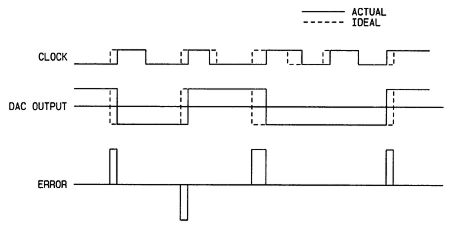
Fig.5 Error due to jitter at the output of a noise-shaping (1-bit) DAC.
Spectrum calculations, however, reveal that 1-bit converters are vastly more sensitive to jitter than are multi-bit converters. The spectral distribution of these pulses after filtering is the convolution product of the (unfiltered) converter output state and jitter spectra. Because the output state of 1-bit converters has a very high noise level just above the audioband (due to noise shaping), the jitter spectrum intermodulates with the converter's noisy output to create audible tones. Because of the large swings in converter output voltage, and because the oversampling multiplier is usually much larger than for conventional converters (64x or 128x vs 8x), noise-shaping converters are much more sensitive to jitter than the conventional ones. In addition, the artifacts are there whether the input signal is large or small, and the 40kHz jitter bandwidth limit no longer applies.
To show how much more sensitive a 1-bit converter is compared to a multi-bit converter, let's take the case of white jitter with a 200ps RMS amplitude applied to the clock of both a 1-bit and a multi-bit converter. In the 1-bit converter, the jitter leads to white noise at the converter output with an approximate amplitude of -75dB in the audio range, regardless of signal amplitude and spectrum. By contrast, the same jitter applied to a clock driving a multi-bit converter creates white noise at -95dB.
Jitter in the digital interface
A logical question to ask is: Where does this clock jitter originate? The main source of jitter is the digital interface between a digital source such as a CD transport and the D/A converter. This interface is either the AES/EBU (Audio Engineering Society/European Broadcast Union) or S/PDIF (Sony/Philips Digital Interface Format) format. With the exception of voltage levels and line impedances, the two formats are very similar. Both carry two channels of digital audio data (up to 24 bits per sample per channel, though only 16 are currently used in consumer applications), control bits, parity bits, and checksum bits. The bit rate is 64 times the sampling frequency (64Fs), and the baud rate (the rate at which the line may change state) is 128Fs. For the CD's 44.1kHz sampling rate, the S/PDIF or AES/EBU interface has a bit rate of 2,822,400 bits per second and a baud rate of 5.6448MHz.
Two optical-fiber interfaces are also in use: TosLink and ST-type, both of which carry information optically instead of electrically. The TosLink interface, more properly called "EIAJ optical," uses a plastic optical fiber. AT&T ST-type optical uses a glass optical fiber. These two optical formats are merely transmission methods; they both use the AES/EBU or S/PDIF data formats.
The digital interface has two major functions: It carries the digital data and it carries the sampling clock. Both data and clock are transmitted on the same physical electrical conductors or optical fiber link: data are encoded using a pulse-modulation scheme, and the clock is embedded in the pulse edges. This system requires that the clock and data be separated in the digital processor, a function performed by the digital processor's input receiver. The "recovered" clock then serves as the processor's master clock. Consequently, jitter in the interface data stream produces clock jitter at the DAC. This is the mechanism by which transports affect a digital system's sonic performance. Moreover, the quality of the digital interface implementation greatly affects the amount of jitter in the recovered clock.
Interface jitter is similar to the periodic clock jitter described earlier. Because current input receiver implementations detect signal edges by comparing the input voltage to zero, jitter in the digital interface signal is defined as the sequence of the timing errors on the voltage zero crossings.
As with noise, jitter has multiple causes. One of them is electrical noise picked up on the interface cable. Noise causes the zero crossing points to shift slightly—which is, by definition, interface jitter. If the digital interface signal has an average slope of 20V/µs (a typical value in many S/PDIF implementations), just 10mV RMS of noise, for example, will introduce 500ps RMS of jitter.
Although noise is a potentially serious cause of interface jitter, bandwidth limitations in the interface are a far greater source. This issue has been described in several articles and papers (footnote 6), but the discussion has been confined to low-pass bandwidth limitations. This article presents the effects of low-pass limitations (that exist in all transmission systems) as well as the effects of high-pass limitations (that occur with all isolation transformers). It is shown that the combined effect of both high-pass and low-pass bandwidth limiting is considerably greater than the effect of either alone.
Let's take the case of two digital signals, A and B, that toggle between a low and a high state. These are shown at the top of fig.6. If these signals are high-pass filtered (as they would be by an isolation transformer), they appear as the waveforms in the center of fig.6. If these signals are also low-pass filtered (as they would be by a digital interface), the waveform assumes the shape at the bottom of fig.6. Note that, at the third transition (marked "3T"), the bandpass filtering causes the edges to have a slope at the zero crossing transition. This slope, combined with the voltage difference, causes a time difference between the zero crossing points of signals A and B. A low-pass filter at 8MHz and a high-pass filter at 50kHz produces a time difference between A and B of 1106ps (1.106ns). By contrast, the low-pass filter alone would produce a timing difference of 2.7ps.
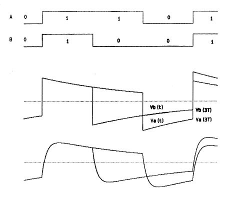
Fig.6 Two perfect digital data signals, A & B (top); waveforms of A & B after passing through typical high-pass filter (middle); waveforms of A & B after passing through typical low-pass and high-pass filter combination (bottom).
While these values apply to a particular segment of the digital interface signal and do not represent the jitter itself, they clearly show the considerable damage caused by a high-pass filter in the data transmission path. Moreover, while increasing the low-pass filter cutoff frequency to 20MHz brings the timing difference caused by the low-pass filter alone to infinitesimal amounts, it only reduces the timing difference caused by the filter combination to 442ps. Clearly, a wide-bandwidth interface is essential for low-jitter transmission of digital audio.
Footnote 6: These include the excellent AES paper, "Is the AES/EBU-S/PDIF Digital Interface Flawed?," by Chris Dunn and Malcolm Omar Hawksford, and the UltraAnalog application note AP-03, "Jitter, jitter, jitter..."—Rémy Fourré
NEXT: Page 3 »
|
| |||||||||
- Log in or register to post comments


| Loudspeakers Amplification Digital Sources | Analog Sources Accessories Featured | Music Columns Retired Columns | Show Reports | Features Latest News Community | Resources Subscriptions |
 © 2024 Stereophile
AVTech Media Americas Inc., USA
All rights reserved