| Columns Retired Columns & Blogs |
Bits is Bits? Page 4
Comparison of Measured Results with Simulations: Using the techniques discussed above, we will now compare the results of simulations with measured results from the experimental interface receiver of fig.4. This circuit allows the instantaneous frequency of the recovered clock to be measured by monitoring the control voltage on the varicap diode. In order to recover the jitter signal on the clock, we must convert the instantaneous frequency signal to a timing error. Consider a frequency deviation Δf in a recovered clock of nominal frequency fo; over a time period dt, the timing error tj can be written:
Footnote 8: AES3-1985, ibid.
Equation 12:
If the measured frequency deviation is sinusoidal, the corresponding jitter frequency is also sinusoidal and of the same frequency, and Δf can be written:
Equation 13:
where:
k = PLL varicap control voltage sensitivity (Hz/V);
V = peak measured voltage on varicap control pin; and
fj = jitter frequency.
Integrating across one quarter-cycle of fj yields the peak jitter tj at this frequency:
Equation 14:
The varicap sensitivity k can be determined by decoupling the PLL feedback loop and monitoring clock frequency under direct control of a DC voltage applied to the control pin. Hence, by measuring the control voltage on the varicap using an analog/digital converter (ADC), and scaling and integrating this signal to follow the law of Equation 14, we have an indirect measure of interface jitter. (Note that although the control voltage in the PLL provides a useful indicator of interface jitter, it will not reveal jitter in the PLL VCO itself above the closed-loop cutoff frequency of the loop, or jitter sources between PLL and converter).
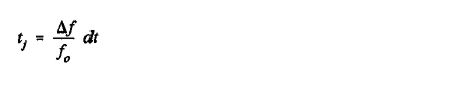
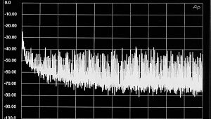
Fig.19a-e shows measured jitter spectra when a DC player's digital output is connected to the experimental interface receiver. The interface signal carries the same audio data in both channels, corresponding to a 1kHz tone at 0dBFS, -20dBFS, -40dBFS, and -60dBFS undithered, and -80.65dBFS dithered, respectively. (These signals were obtained using the Hi-Fi News & Record Review Test Disc 2.) Each jitter spectrum consists of a large fundamental harmonic of the audio signal as well as higher harmonics and noise superimposed upon the frequency response of the PLL loop filter. Note the changes in the relative magnitudes of the harmonics, as well as the absolute jitter level, as the magnitude of the audio signal changes.
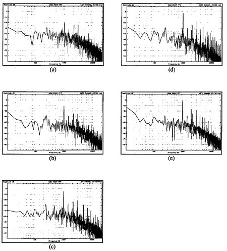
Fig.19 Measured jitter spectra at interface receiver for 1kHz audio signals at a) 0dBFS, b) -20dBFS, c) -40dBFS, d) -60dBFS, and e) -80.65dBFS.
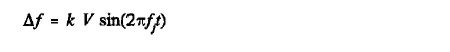
These measured results can be directly compared to simulations of the recovered clock-jitter spectra for the same audio signals (fig.20a-e). The simulations were obtained using the theory developed in "Interface Bandwidth Limitation" (above), with a minor change: the average jitter model outlined above calculates the jitter based on interface signal transitions at every cell edge, while the Philips SAA7274 ADIC employed in the experimental receiver controls the PLL via timing errors at each negative-going transition. The simulation software was adjusted accordingly. Results were obtained using an interface time constant of 65ns and a first-order PLL loop filter with break frequency set to 1kHz.
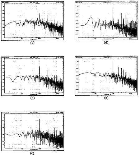
Fig.20 Simulated interface jitter spectra for interface time constant of 65ns and a 1kHz audio signals at a) 0dBFS, b) -20dBFS, c) -40dBFS, d) -60dBFS, and e) -80.65dBFS.
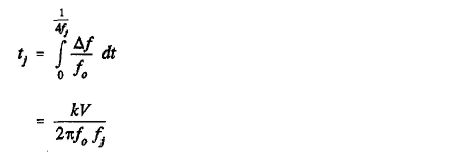
In general, the simulations show good agreement with the measured results; the only discrepancies appear as low-level tones in the measured jitter spectra at 230Hz, 1.6kHz, and 2.1kHz. These tones are also present in a jitter measurement taken while no CD was playing, but while the receiver was still locked to the digital interface signal (fig.21). These frequencies are due to factors not taken into account in the software model: the first frequency can be accounted for by considering the change in the subframe preamble when a channel status block begins every 192 frames (footnote 8); it is possible that the 1.6kHz and 2.1kHz components are jitter artifacts inherent to the ADIC employed.
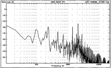
Fig.21 Measured jitter spectrum with receiver locked but no CD playing
Finally, fig.22 shows the jitter noisefloor of the measurement system, obtained with the input of the ADC connected to ground (note the expanded amplitude scale in this diagram). The low level of jitter in this measurement indicates that the measurement system employed has not compromised the accuracy of the results obtained above.
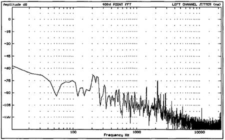
Fig.22 Jitter measurement noise floor.
The good agreement achieved between practice and theory allows us to make predictions about the audibility of jitter errors in conversion electronics, based upon the band-limited interface jitter model developed above. An important result to note from the measurements is the high degree of correlation that can occur between audio and jitter signals. It is instructive to audition the PLL control voltage in an interface receiver after suitable amplification; the audio signal transmitted over the interface can be clearly heard (although it is noisy and highly distorted) as the PLL attempts to track jitter on the received interface signal (a phenomenon also reported by van Willenswaard (footnote 9).
The authors have found that track 2 of the Hi-Fi News & Record Review Test Disc 2 is particularly useful in this experiment, since it includes sections where identical signals are recorded in and out of phase across two stereo channels. The in-phase version is heard as a much louder signal at the PLL control voltage, since the PCM twos-complement-coded out-of-phase signal has a zero Zero-One sum across one interface frame. A clock used in an A/D or D/A conversion process that suffers from jitter that is highly correlated with the audio signal can cause distortion tones that are audibly more objectionable than noise modulation that would otherwise occur for noise-like jitter. (See "Audibility of Jitter Errors.")
The measured results for the experimental interface imply a time constant of about 65ns. This is interesting in that the interface signal used in the experiments exhibited risetimes in the order of 10ns at the receiver input when observed using a high-bandwidth oscilloscope. However, a band-limitation at any stage in the interface will cause jitter in the embedded clock signal, even if the interface signal-transition edges are subsequently cleaned up. Every stage in the interface—transmitter, link, and receiver—is a possible source of band-limitation, and thus jitter. We believe that an equivalent time constant of 65ns within the ADIC IC was responsible for the jitter observed in the experiments.
Footnote 8: AES3-1985, ibid.
Footnote 9: Peter van Willenswaard, Stereophile, November 1990, Vol.13 No.11, pp.78-83.
NEXT: Page 5 »
|
| |||||||||
- Log in or register to post comments


| Loudspeakers Amplification Digital Sources | Analog Sources Accessories Featured | Music Columns Retired Columns | Show Reports | Features Latest News Community | Resources Subscriptions |
 © 2024 Stereophile
AVTech Media Americas Inc., USA
All rights reserved